TS13002HV
Overview
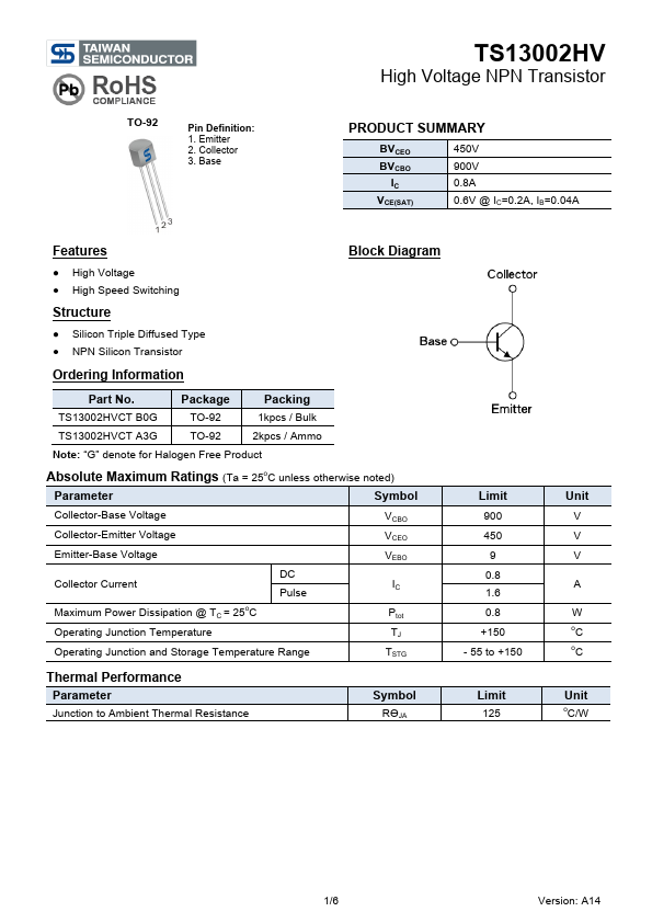
TS13002HV High Voltage NPN Transistor TO-92 Pin Definition: 1. Emitter 2. Collector 3. Base PRODUCT SUMMARY BVCEO BVCBO IC VCE(SAT) 450V 900V 0.8A 0.6V @ IC=0.2A, IB=0.04A Features Block Diagra...
| Part | TS13002HV |
|---|---|
| Description | High Voltage NPN Transistor |
| Category | Transistor |
| Manufacturer | Taiwan Semiconductor |
| Size | 648.28 KB |
TS13002HV High Voltage NPN Transistor TO-92 Pin Definition: 1. Emitter 2. Collector 3. Base PRODUCT SUMMARY BVCEO BVCBO IC VCE(SAT) 450V 900V 0.8A 0.6V @ IC=0.2A, IB=0.04A Features Block Diagra...
| Part Number | Manufacturer | Description |
|---|---|---|
| 13007B | TSC | TS13007B |
| TS13003 | Taiwan Semiconductor | High Voltage NPN Transistor |
| TS13003B | Taiwan Semiconductor | High Voltage NPN Transistor |
| TS13003MV | Taiwan Semiconductor | High Voltage NPN Transistor |
| TS13003HV | Taiwan Semiconductor | High Voltage NPN Transistor |